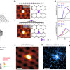
Crystals can have defects at the nanometre scale, which may affect the thermal and heat transport properties of crystalline materials used in a variety of high-technology devices. Employing newly developed electron microscopy techniques, researchers at the University of California, Irvine (UCI) and other institutions have, for the first time, measured the spectra of phonons at individual crystalline faults, and they discovered the propagation of phonons near the flaws.
“Point defects, dislocations, stacking faults and grain boundaries are often found in crystalline materials, and these defects can have a significant impact on a substance’s thermal conductivity and thermoelectric performance”, said senior co-author Xiaoqing Pan from UCI.
He said that there are ample theories to explain the interactions between crystal imperfections and phonons, but little experimental validation due to the inability of earlier methods to view the phenomena at high enough space and momentum resolution. Pan and his collaborators approached the problem through the novel development of space- and momentum-resolved vibrational spectroscopy in a transmission electron microscope at UCI’s Irvine Materials Research Institute.
With this technique, they were able to observe individual defects in cubic silicon carbide, a material with a wide range of applications in electronic devices. Pan and his colleagues were familiar with how imperfections in silicon carbide are manifested as stacking faults, and theoretical work has described the thermoelectric impacts, but now the team has produced direct experimental data to characterise phonon interactions with the individual defects.
“Our method opens up the possibility of studying the local vibrational modes at intrinsic and non-intrinsic defects in materials”, said Pan. “We expect it to find important applications in many different areas, ranging from the study of thermal resistance-inducing interfacial phonons to defect structures engineered to optimise a material’s thermal properties.”


